|
View this message online
|
|
|
|
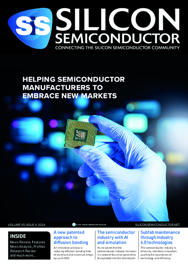
Silicon Semiconductor Magazine - 2025 Issue 1 - Part 1
|
|
|
|
|

|
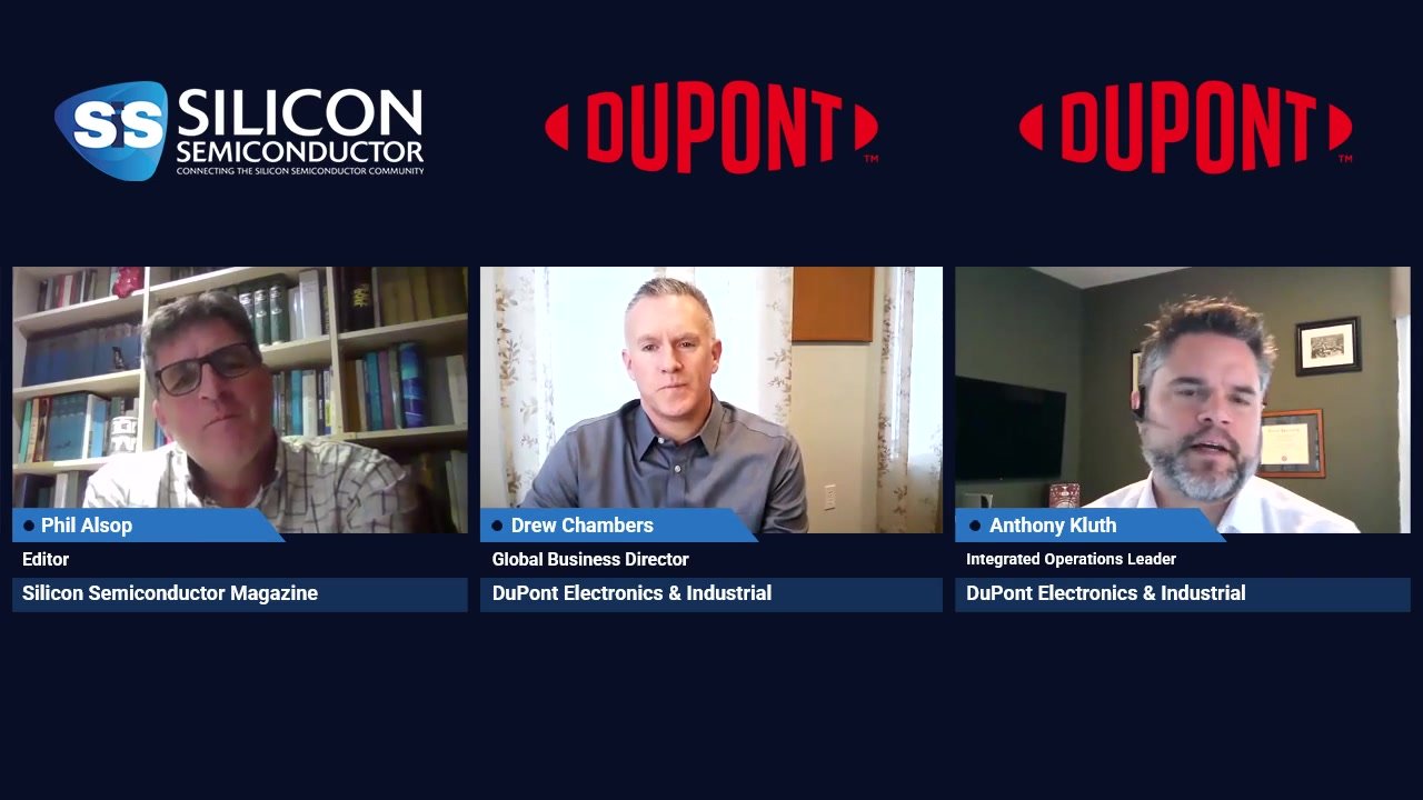
Drew Chambers, Global Business Director and Anthony Kluth, Integrated Operations Leader, both at Lithography Technologies, Semiconductor Technologies, DuPont Electronics & Industrial, talk through the logistics and benefits of a significant expansion for photoresist manufacturing capacity at the company’s Sasakami site in Japan, going on to share insights as to the EUV lithography challenges and opportunities on which DuPont is currently focused, alongside its work to address substances of concern. Anthony and Drew also share their thoughts on DuPont’s and the wider semiconductor industry’s future, with sustainability, supply chain, skills and the company’s roadmap discussed.
|
|
|
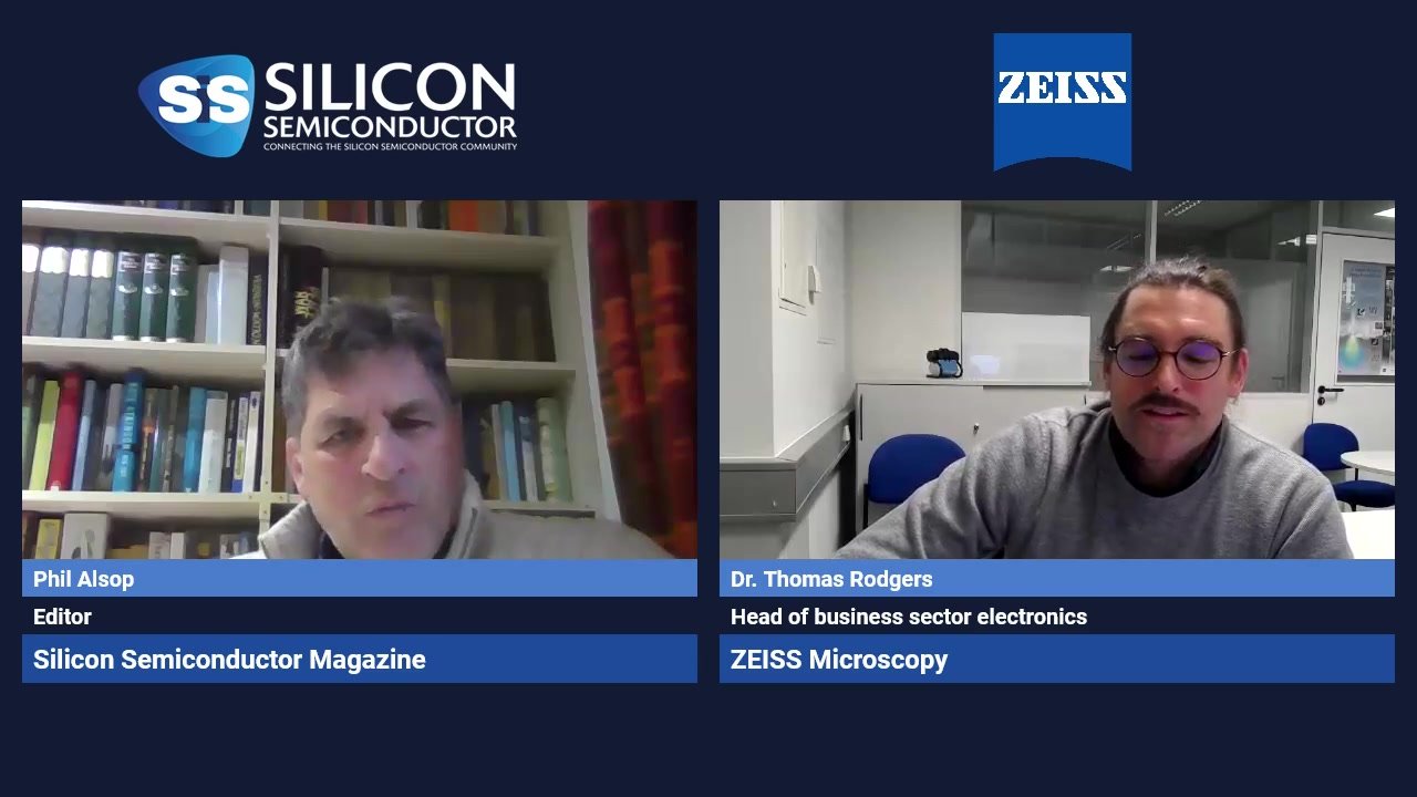
Dr. Thomas Rodgers, head of business sector electronics at ZEISS Microscopy, talks through the company’s new ZEISS Crossbeam 550 Samplefab. Built for efficiency and throughput in the semiconductor lab, ZEISS Crossbeam 550 Samplefab provides recipe-based automation for the routine TEM sample preparation work of bulk milling, lift-out and thinning at any number of target points on the sample. The solution promises an automation yield of >90% for processing lamellae from bulk to TEM grid without operator intervention.
|
|
|
Nick New, CEO of Optalysys, explains how the company enables the future of secure compute by processing encrypted data at scale, without it being decrypted. It does this by using the power of advanced silicon photonics to enable Fully Homomorphic Encryption, a cryptographic technology to allow organisations to securely commercialise their data, providing several significant advantages to traditional electronic semiconductors.
|
|
|
Hamed Sadeghian, CEO of Nearfield Instruments, discusses a recent purchase order win for the company’s flagship QUADRA High-Throughput Process Control Metrology product. The order, secured after an intensive supplier selection process, was placed by a prominent semiconductor manufacturer in East Asia, further strengthening Nearfield Instruments’ presence in this technologically advanced region.
|
|
|
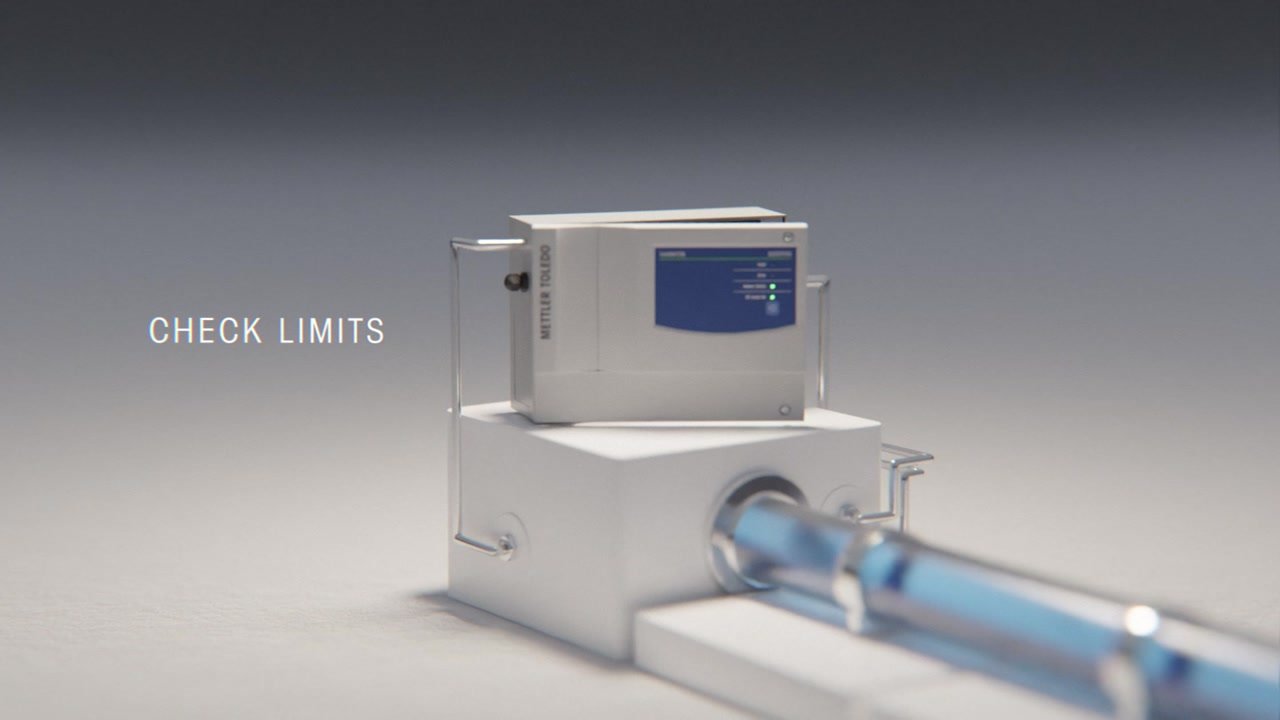
Waste reduction and water use are two major issues affecting the semiconductor industry, and facilities are looking for ways to improve sustainability and water reclaim. METTLER TOLEDO’s on-line water analytics solutions for conductivity, TOC, microbial detection, pH, and dissolved oxygen help monitor water purity in wafer manufacturing and reclaim/reuse processes to minimize rejected wafers and maximize water recovery.
|
|
|
|
Next opportunity
|
|
One of the major successes for clients of Silicon Semiconductor Magazine has been our recorded ZOOM interviews. With an average audience of well over 1000 viewers per interview, we can see how well appreciated they are by our readership. We will be happy to set up an interview and ensure that your company's announcements receive the recognition they deserve.
|
|
Package details
|
30 Minutes
£995
|
30 min ZOOM interview with the editor
The interview will include a single page of advertising in Silicon Semiconductor or 1 Newsletter sponsorship. Package Price £995
|
|
|
Contact us
|
|
|
|
Recent issues of Silicon Semiconductor Magazine
|
|
|
| |
|
|
We hope that you found this message of interest. If not, you may easily unsubscribe or manage your preferences.
[COMPANY_ADDRESS]

|
|